- 您现在的位置:买卖IC网 > Sheet目录332 > IR2235JPBF (International Rectifier)IC DRIVER BRIDGE 3PHASE 44PLCC
IR2133/IR2135/IR2233 / IR2235(J & S )&(PbF)
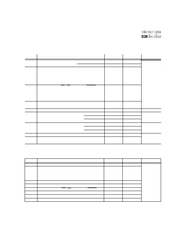
Absolute Maximum Ratings
Absolute Maximum Ratings indicate sustained limits beyond which damage to the device may occur. All volt-
age parameters are absolute voltages referenced to COM. The Thermal Resistance and Power Dissipation
ratings are measured under board mounted and still air conditions.
Symbol
Definition
Min.
Max.
Units
V B1,2,3
High side floating supply voltage
(IR2133/IR2135)
(IR2233/IR2235)
-0.3
-0.3
625
1225
V S1,2,3
V HO1,2,3
V CC
High side floating supply offset voltage
High side floating output voltage
Fixed supply voltage
V B1,2,3 - 25
V S1,2,3 - 0.3
-0.3
V B1,2,3 + 0.3
V B1,2,3 + 0.3
25
V SS
V LO1,2,3
V IN
Logic ground
Low side output voltage
Logic input voltage (HIN, LIN, ITRIP, SD & FLT-CLR)
V CC - 25
-0.3
V SS - 0.3
V CC + 0.3
V CC + 0.3
(V SS + 15) or
V
(V CC + 0.3)
whichever is
lower
V IN,AMP
V OUT,AMP
V FLT
Op amp input voltage (CA+ & CA-)
Op amp output voltage (CAO)
FAULT output voltage
V SS - 0.3
V SS - 0.3
V SS - 0.3
V CC + 0.3
V CC + 0.3
V CC + 0.3
dV S /dt
P D
Rth JA
T J
T S
T L
Allowable offset supply voltage transient
Package power dissipation @ T A ≤ 25oC (28 Lead PDIP)
(28 Lead SOIC)
(44 lead PLCC)
Thermal resistance, junction to ambient (28 Lead PDIP)
(28 Lead SOIC)
(44 lead PLCC)
Junction temperature
Storage temperature
Lead temperature (soldering, 10 seconds
—
—
—
—
—
—
—
—
-55
—
50
1.5
1.6
2.0
83
78
63
125
150
300
V/ns
W
oC/W
oC
Recommended Operating Conditions
The input/output logic timing diagram is shown in figure 1. For proper operation the device should be used within the
recommended conditions. All voltage parameters are absolute voltages referenced to COM. The VS offset rating is
tested with all supplies biased at 15V differential.
Symbol Parameter Definition
Min.
Max.
Units
V B1,2,3
V S1,2,3
High side floating supply voltage
High side floating supply offset voltage (IR2133/IR2135)
(IR2233/IR2235)
V S1,2,3 + 10/12 V S1,2,3 + 20
Note 1 600
Note 1 1200
V HO1,2,3
High side floating output voltage
V S1,2,3
V B1,2,3
V CC
Fixed supply voltage
10 or 12 20
V SS
V LO1,2,3
Low side driver return
Low side output voltage
-5 5
0 V CC
V
V IN
V IN,AMP
V OUT,AMP
V FLT
Logic input voltage (HIN, LIN, ITRIP, SD & FLT-CLR)
Op amp input voltage (CA+ & CA-)
Op amp output voltage (CAO)
FAULT output voltage
V SS
V SS
V SS
V SS
V SS + 5
V SS + 5
V SS + 5
V CC
Note 1: Logic operational for VS of COM - 5V to COM + 600V/1200V. Logic state held for VS of COM -5V to COM -VBS. (Please refer to the Design Tip
DT97-3 for more details).
Note 2: All input pins, op amp input and output pins are internally clamped with a 5.2V zener diode.
2
www.irf.com
发布紧急采购,3分钟左右您将得到回复。
相关PDF资料
IR2301PBF
IC DRIVER HIGH/LOW SIDE 8DIP
IR2302PBF
IC DRIVER HALF BRIDGE 8DIP
IR2304SPBF
IC DRIVER HALF BRIDGE 8-SOIC
IR2308SPBF
IC DRIVER HALF BRIDGE HV 8SOIC
IR3101
IC POWER MODULE 1.6A 500V 11-SIP
IR3103
PWR MOD 180W GATE DRIVER 11-SIP
IR3519STRPBF
IC MOSFET GATE DRIVER SON-8
IR4427STRPBF
IC DRIVER DUAL LOW SIDE 8SOIC
相关代理商/技术参数
IR2235JTR
功能描述:IC DRIVER 3-PHASE BRIDGE 44-PLCC RoHS:否 类别:集成电路 (IC) >> PMIC - MOSFET,电桥驱动器 - 外部开关 系列:- 标准包装:50 系列:- 配置:高端 输入类型:非反相 延迟时间:200ns 电流 - 峰:250mA 配置数:1 输出数:1 高端电压 - 最大(自引导启动):600V 电源电压:12 V ~ 20 V 工作温度:-40°C ~ 125°C 安装类型:通孔 封装/外壳:8-DIP(0.300",7.62mm) 供应商设备封装:8-DIP 包装:管件 其它名称:*IR2127
IR2235JTRPBF
功能描述:功率驱动器IC 3Phs Drvr Sep Hi&Lw Side Input 200ns RoHS:否 制造商:Micrel 产品:MOSFET Gate Drivers 类型:Low Cost High or Low Side MOSFET Driver 上升时间: 下降时间: 电源电压-最大:30 V 电源电压-最小:2.75 V 电源电流: 最大功率耗散: 最大工作温度:+ 85 C 安装风格:SMD/SMT 封装 / 箱体:SOIC-8 封装:Tube
IR2235PbF
功能描述:功率驱动器IC 3-Phase Bridge DRVR 600V 200mA 250ns RoHS:否 制造商:Micrel 产品:MOSFET Gate Drivers 类型:Low Cost High or Low Side MOSFET Driver 上升时间: 下降时间: 电源电压-最大:30 V 电源电压-最小:2.75 V 电源电流: 最大功率耗散: 最大工作温度:+ 85 C 安装风格:SMD/SMT 封装 / 箱体:SOIC-8 封装:Tube
IR2235S
功能描述:IC DRIVER 3-PHASE BRIDGE 28-SOIC RoHS:否 类别:集成电路 (IC) >> PMIC - MOSFET,电桥驱动器 - 外部开关 系列:- 标准包装:50 系列:- 配置:低端 输入类型:非反相 延迟时间:40ns 电流 - 峰:9A 配置数:1 输出数:1 高端电压 - 最大(自引导启动):- 电源电压:4.5 V ~ 35 V 工作温度:-40°C ~ 125°C 安装类型:表面贴装 封装/外壳:TO-263-6,D²Pak(5 引线+接片),TO-263BA 供应商设备封装:TO-263 包装:管件
IR2235SPbF
功能描述:功率驱动器IC 3 PHASE DRVR HI & LO SIDE INPUTS RoHS:否 制造商:Micrel 产品:MOSFET Gate Drivers 类型:Low Cost High or Low Side MOSFET Driver 上升时间: 下降时间: 电源电压-最大:30 V 电源电压-最小:2.75 V 电源电流: 最大功率耗散: 最大工作温度:+ 85 C 安装风格:SMD/SMT 封装 / 箱体:SOIC-8 封装:Tube
IR2235STRPBF
功能描述:功率驱动器IC 3 PHASE DRVR HI & LO SIDE INPUTS RoHS:否 制造商:Micrel 产品:MOSFET Gate Drivers 类型:Low Cost High or Low Side MOSFET Driver 上升时间: 下降时间: 电源电压-最大:30 V 电源电压-最小:2.75 V 电源电流: 最大功率耗散: 最大工作温度:+ 85 C 安装风格:SMD/SMT 封装 / 箱体:SOIC-8 封装:Tube
IR2237
制造商:IRF 制造商全称:International Rectifier 功能描述:3-PHASE BRIDGE DRIVER
IR2237J
制造商:IRF 制造商全称:International Rectifier 功能描述:3-PHASE BRIDGE DRIVER
